In a major breakthrough, IBM scientists have placed and tested more than 10,000 carbon nanotube devices in a single chip, using mainstream manufacturing processes. This could pave the way for carbon nanotubes as a viable alternative to silicon in future computing – allowing Moore's Law to continue for some time to come.
 |
| Carbon nanotube breakthrough by IBM could lead to the next generation of computer chips |
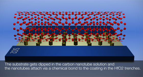
IBM researchers have demonstrated a new approach to carbon nanotechnology that opens up the path for commercial fabrication of dramatically smaller, faster and more powerful computer chips. For the first time, more than 10,000 working transistors made of nano-sized tubes of carbon have been precisely placed and tested in a single chip using standard semiconductor processes. These carbon devices are poised to replace and outperform silicon, allowing further miniaturisation of computing components.
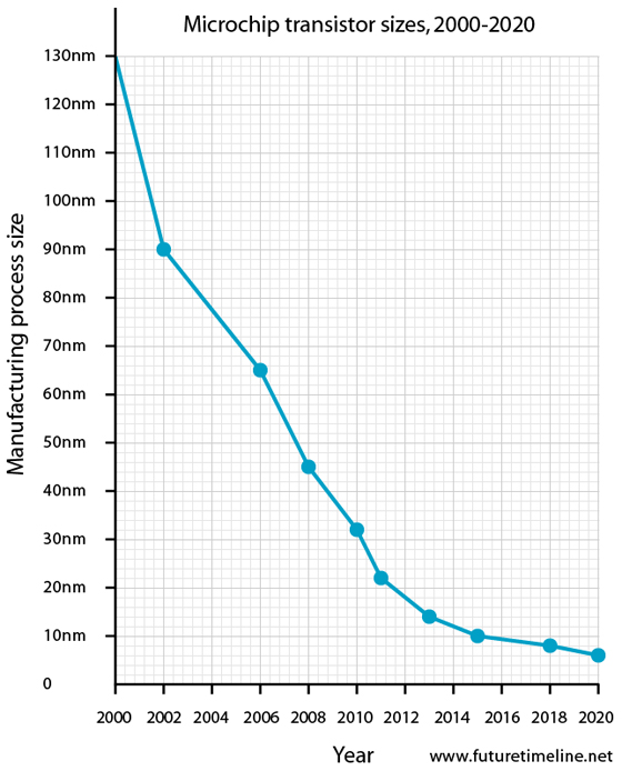
Aided by rapid innovation over four decades, silicon microprocessor technology has continually shrunk in size and improved in performance, thereby driving the information technology revolution. Silicon transistors – tiny switches that carry information on a chip – have been made smaller year after year, but they are approaching a point of physical limitation. Their increasingly small dimensions, now reaching the nanoscale, will prohibit any gains in performance due to the nature of silicon and the laws of physics. Within a few more generations, classical scaling and shrinkage will no longer yield the sizable benefits of lower power, lower cost and higher speed processors that the industry has become accustomed to.

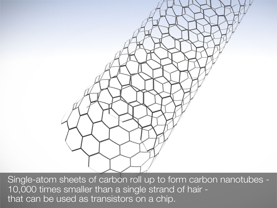
Carbon nanotubes represent a new class of semiconductor materials whose electrical properties are more attractive than silicon, particularly for building nanoscale transistor devices that are a few tens of atoms across. Electrons in carbon transistors can move easier than in silicon-based devices allowing for quicker transport of data. The nanotubes are also ideally shaped for transistors at the atomic scale, an advantage over silicon. These qualities are among the reasons to replace the traditional silicon transistor with carbon – and coupled with new chip design architectures – will allow computing innovation on a miniature scale for the future.
The approach developed at IBM paves the way for circuit fabrication with large numbers of carbon nanotube transistors at predetermined substrate positions. The ability to isolate semiconducting nanotubes and place a high density of carbon devices on a wafer is crucial to assess their suitability for a technology – eventually over a billion transistors will be needed for future integration into commercial chips. Until now, scientists have been able to place at most a few hundred carbon nanotubes at a time, not nearly enough to address key issues for commercial applications.

Supratik Guha, Director of Physical Sciences at IBM Research: “Carbon nanotubes, borne out of chemistry, have largely been laboratory curiosities as far as microelectronic applications are concerned. We are attempting the first steps towards a technology by fabricating carbon nanotube transistors within a conventional wafer fabrication infrastructure. The motivation to work on carbon nanotube transistors is that at extremely small nanoscale dimensions, they outperform transistors made from any other material. However, there are challenges to address such as ultra high purity of the carbon nanotubes and deliberate placement at the nanoscale. We have been making significant strides in both.”
Study co-author James Hannon, a materials scientist at IBM, says there are few realistic successors to silicon: "The problem is you have to put it into production on a 10- or 15-year time scale, so the kinks have to be worked out in the next few years."
Originally studied for the physics that arises from their atomic dimensions and shapes, carbon nanotubes are being explored by scientists worldwide in applications ranging from integrated circuits, to energy storage, biomedical sensing and DNA sequencing.
IBM's breakthrough is published in the peer-reviewed journal Nature Nanotechnology.
Post a Comment